In the previous segment, we went through the process for taking Gcode, and sending it through
to produce the final circuit boards. This section will discuss the process for Generating that
Gcode. So far the best option for designing a PCB layout is Autodesk Eagle, it is surprisingly
versatile, and allows you to import Libraries made by other people, which can help with specific
component footprints. The only downside is that there is a learning curve about as steep as a
brick wall, so it might help to play around with it, even I am still not used to it.
First, Install autodesk Eagle, and hope that your wifi is strong enough, because this one will
take some time. After that is done, open and start Eagle, you'll be met with this menu.
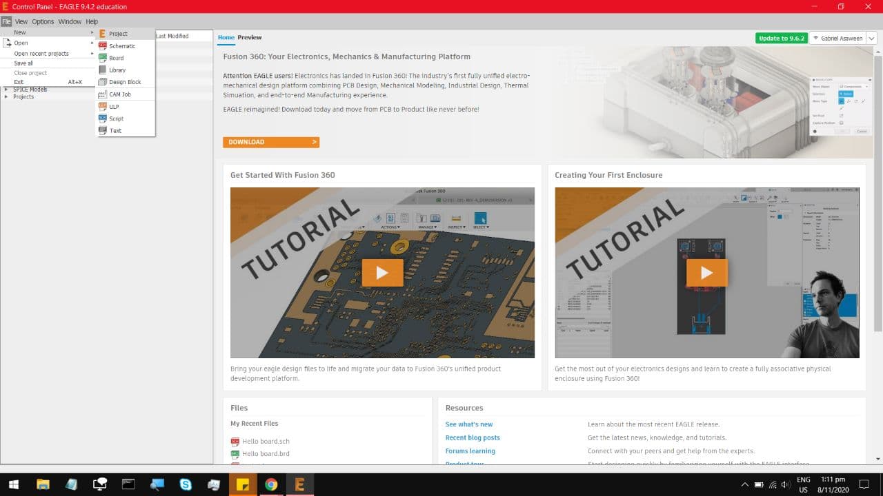
Next, select file, new, project.
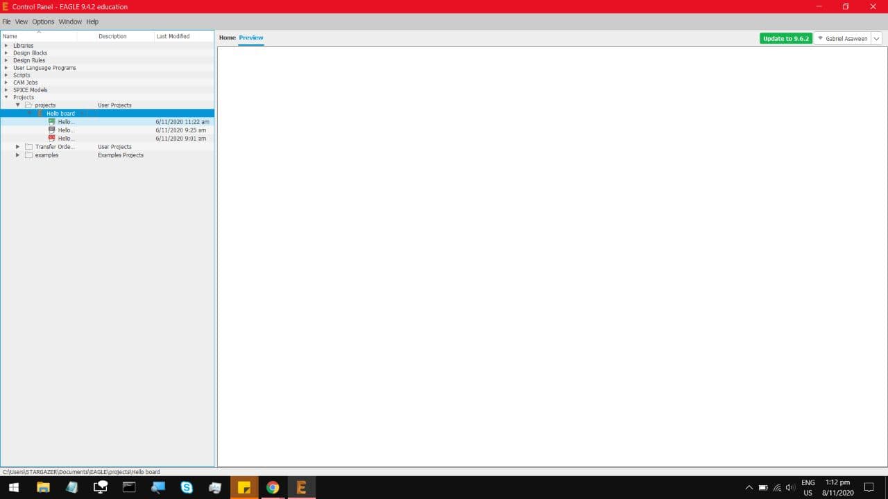
And it brings you to the projects tab. From here you can select your libraries and projects to work on.
Right Click on your project, and select New Schematic.
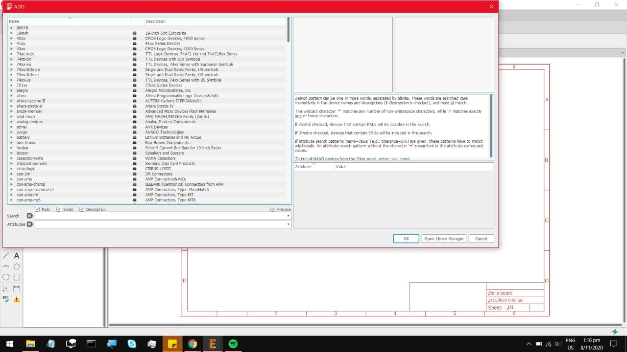
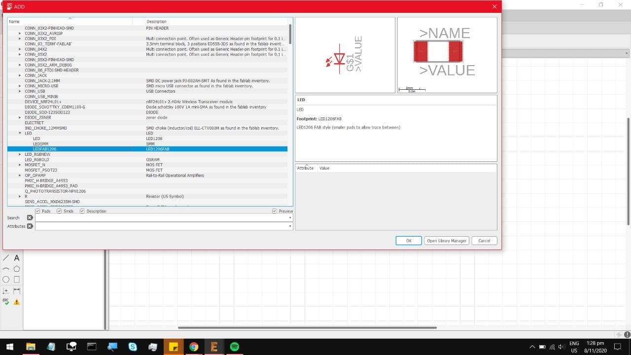
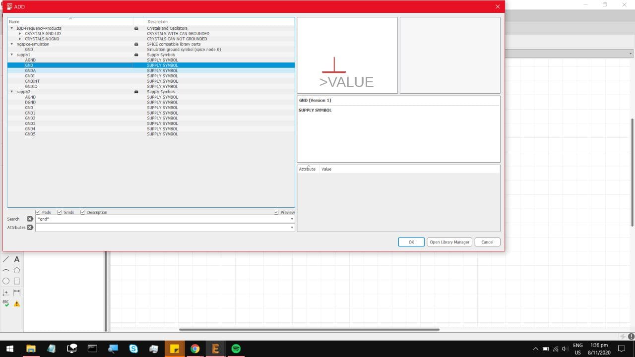
And this brings you to the schematic, from her select Edit, Add.
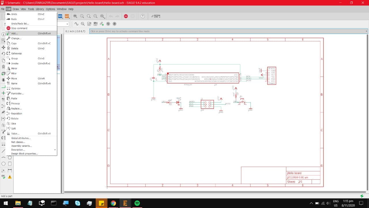
This is where you can add various components. For this I will use a Library from the FabLab, as its got the SMD
components that are available to us.
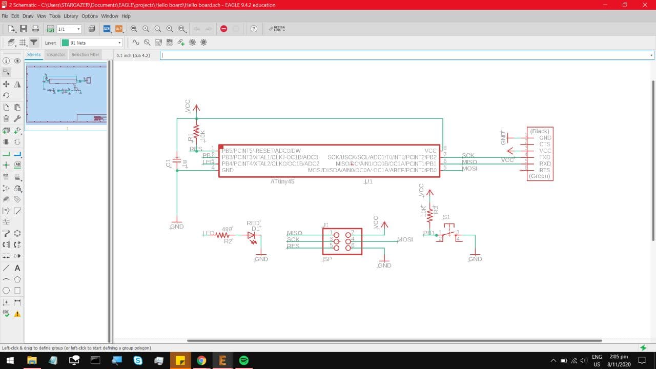
For demonstration on how to use this software, I will make a circuit that does absolutely nothing
just to keep things simple. If we take this capacitor, it shows us the circuit symbol, but more importantly
it shows us the Package footprint, which is great for figuring out which specific components to use.
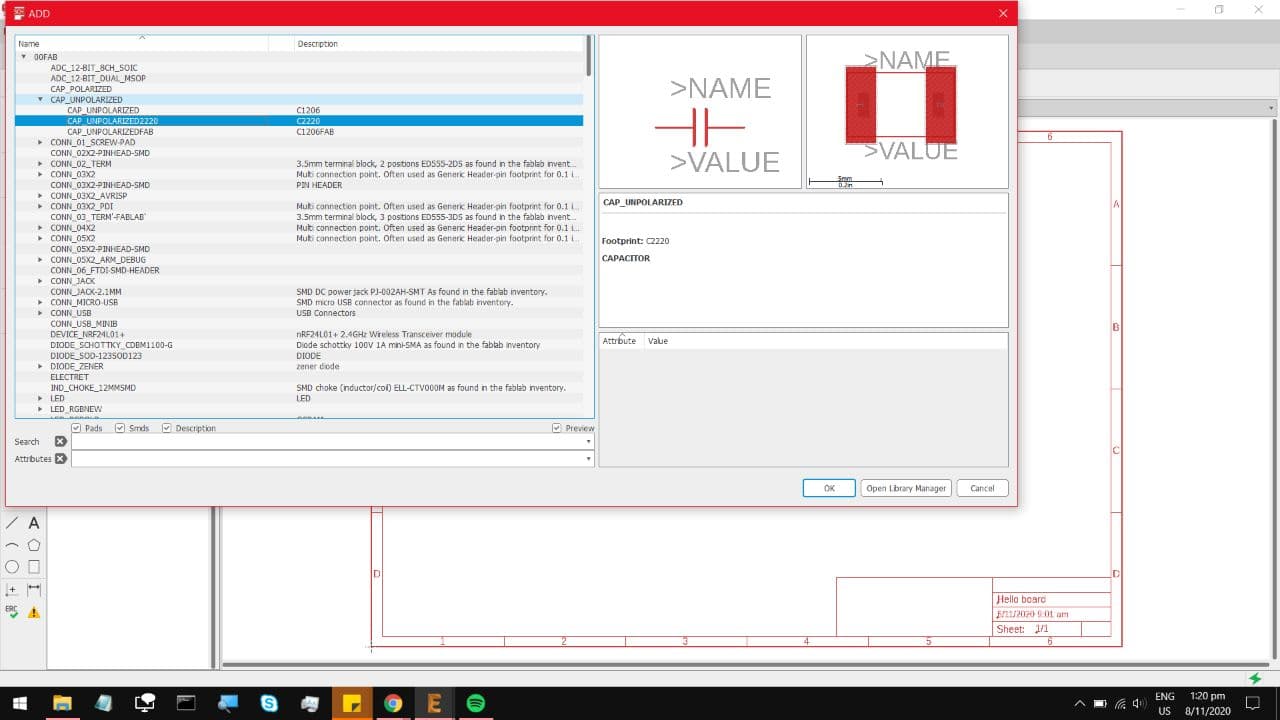
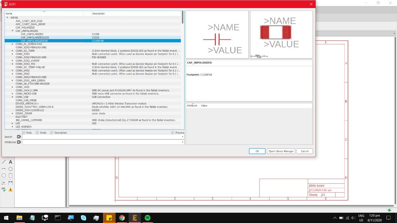
Alternatively, we have this capacitor with a much smaller footprint, lets use this one. Right click to rotate the component.
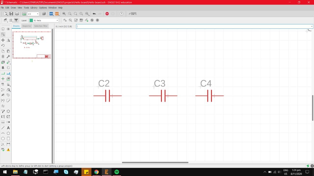
Hit okay and drop as many as you'd like into the schematic. To make things easier, there is a button
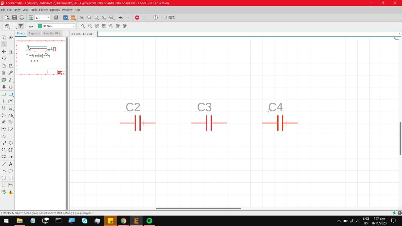
under the save icon. This is to toggle a Grid, so select the grid size, and hit Display On, and Ok.
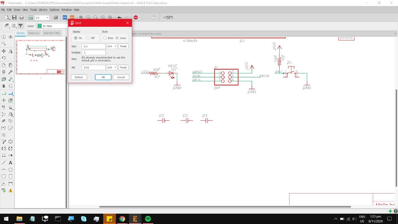
This grid is surprisingly useful when it comes to alignment. Now if you zoom in you will notice there is a tiny
red cross on the component symbol, if you click and hold that red cross, you can move the component around, its
easy to spot here but for some of the larger ICs its almost impossible to find unless your brightness is at 100.
If you click the the component to select it, it will appear 1 percent more Red than the others. Alternatively
you can Ctrl+A to select all, or even highlight it with the mouse. Its at this point you should know, working this
with a Laptop is just incredibly frustrating, much like every other Autodesk softwares.
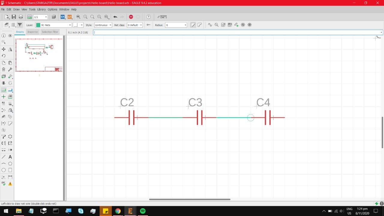
On the Left edge, theres a tool highlighted with a Green L icon, that is your routing,
to match component connections, where you can add circuit pathways.
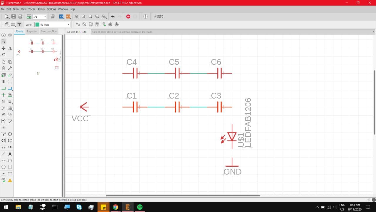
Now let's throw some other stuff in. You'll notice that LEDs have a very similar package footprint to Capacitors
or resistors, so it is very important to Label your components, which will make the next few steps less frustrating.
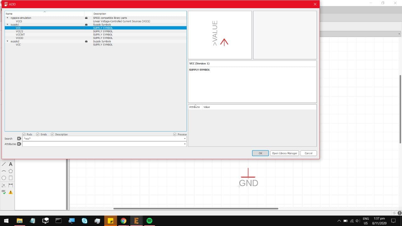
And for Ground connections and VCC you can search it in the search bar.
So we have this basic layout, you can highlight whole circuits over and Ctrl+C Ctrl+V,
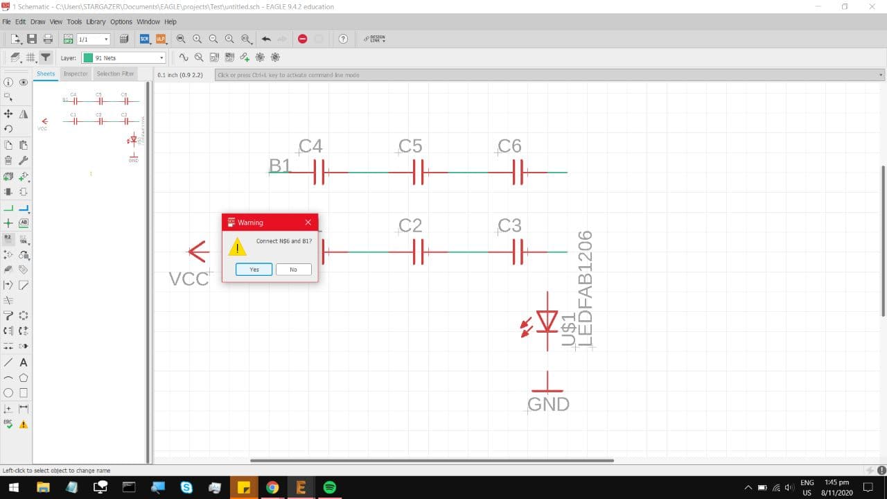
Now here is a neat trick for complex circuits, if you extend a small route and Label it, something like B1
and label another connection as B1 as well like this.
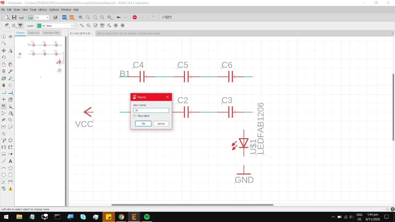
You will be prompted with this that asks to Connect the two points, Click Ok.
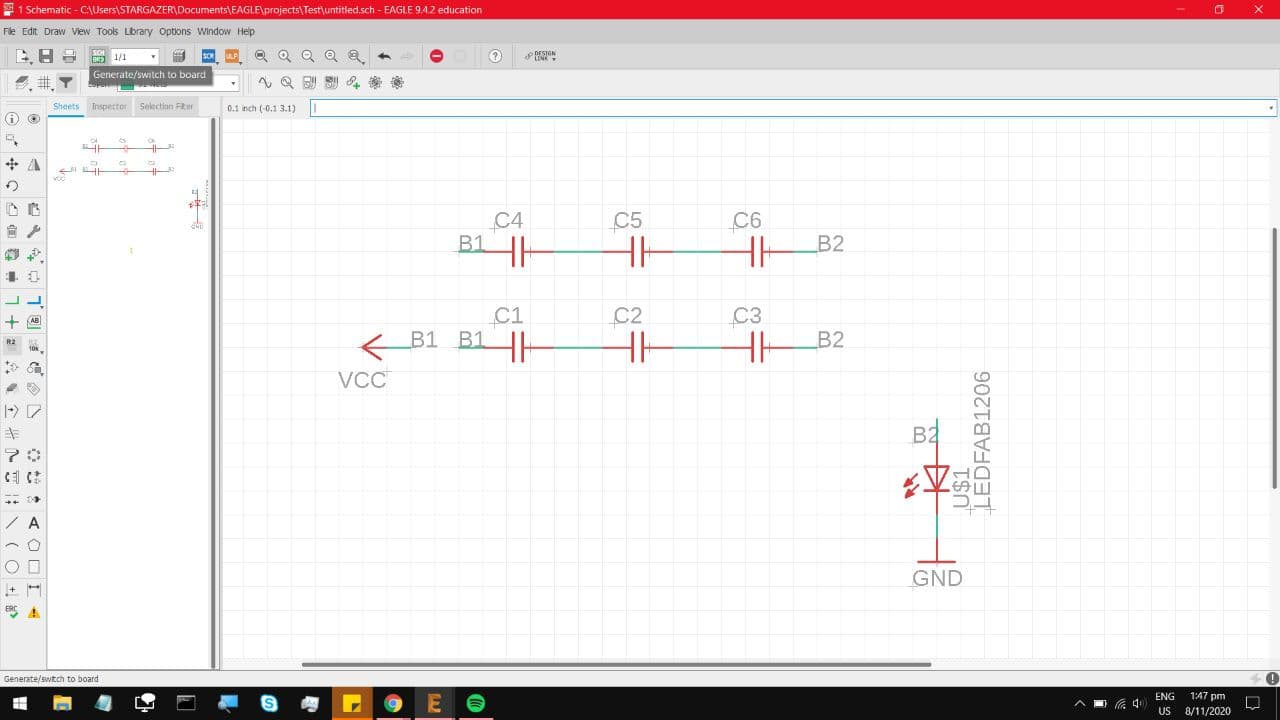
So that leaves us with this layout. On the top there is a button highlighted, that will switch over to the Board layout.
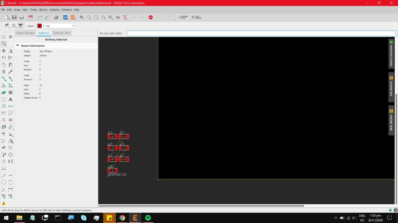
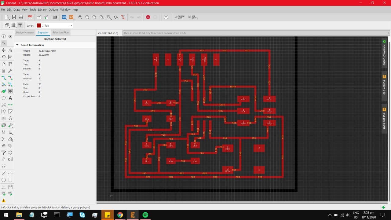
And this is the main board layout. First thing, do not Ctrl+A here as it will also select and move the Origin positon.
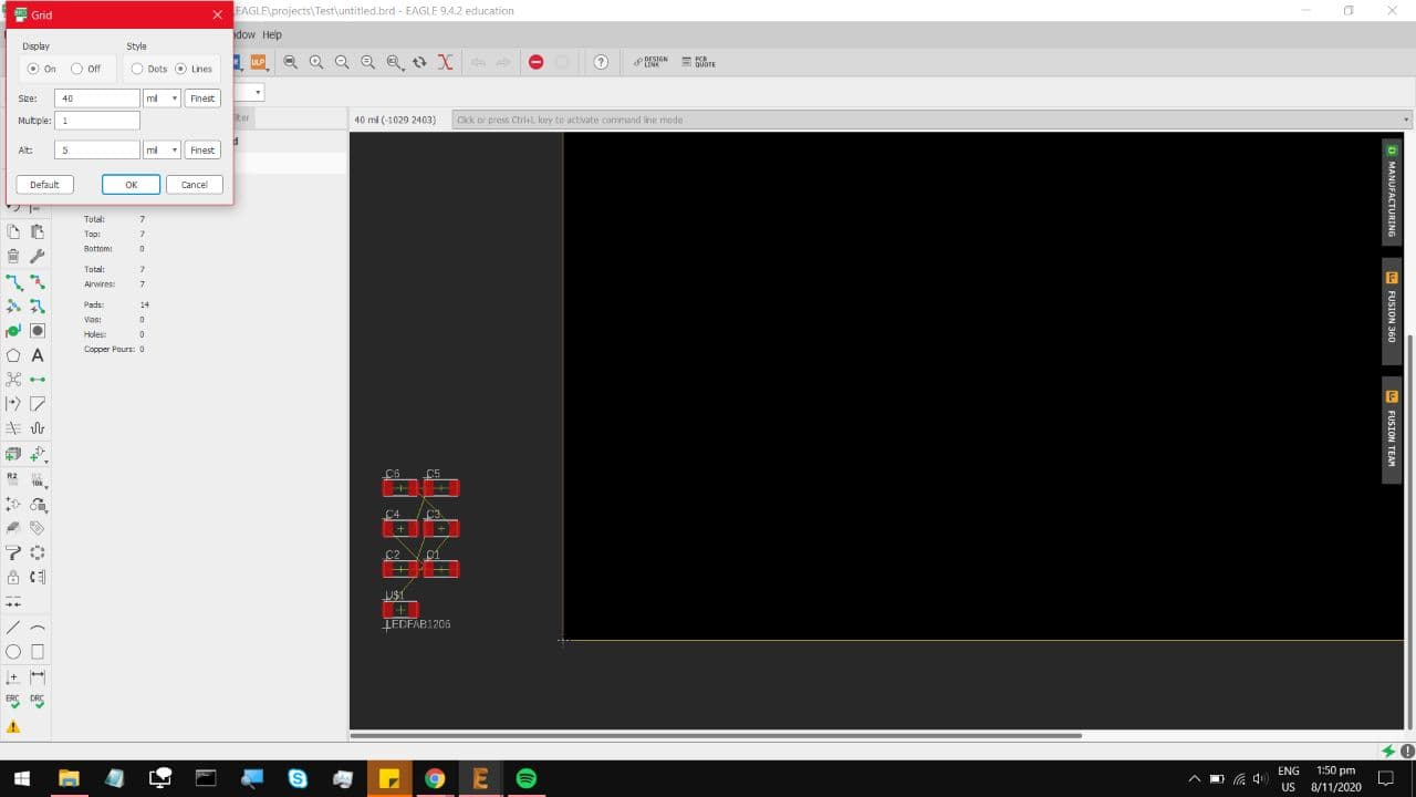
Once again, set up a grid layout to make things easier to align,
You can highlight and move all of the components. Those yellow lines between the components are the
circuit connections, otherwise known as a Ratsnest for..obvious reasons. First we have to Untangle
that, and this is exactly why Labelling matters here, Because every component here looks the same.
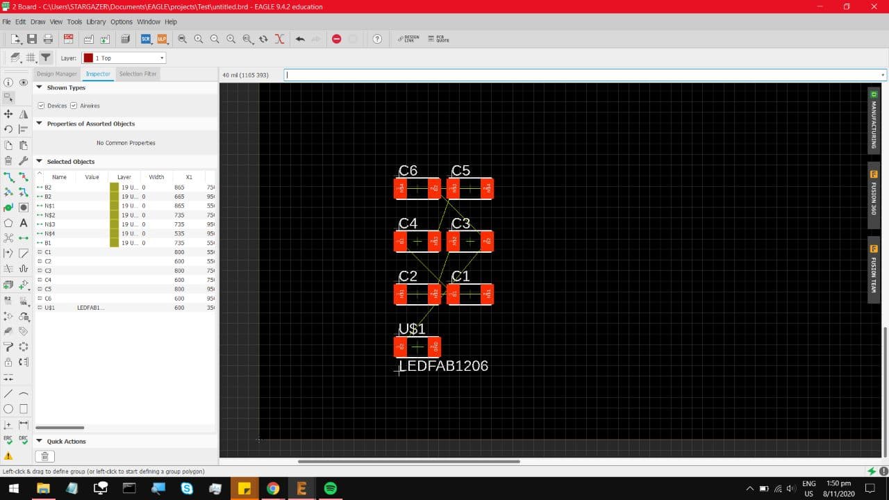
Now that we have this untangled, by physically moving and rotating components around, you notice that
C6 and C3 are connected, as are C4 and C1, even though they were not connected in the schematic.
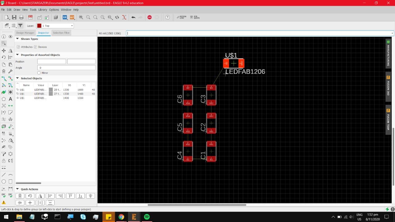
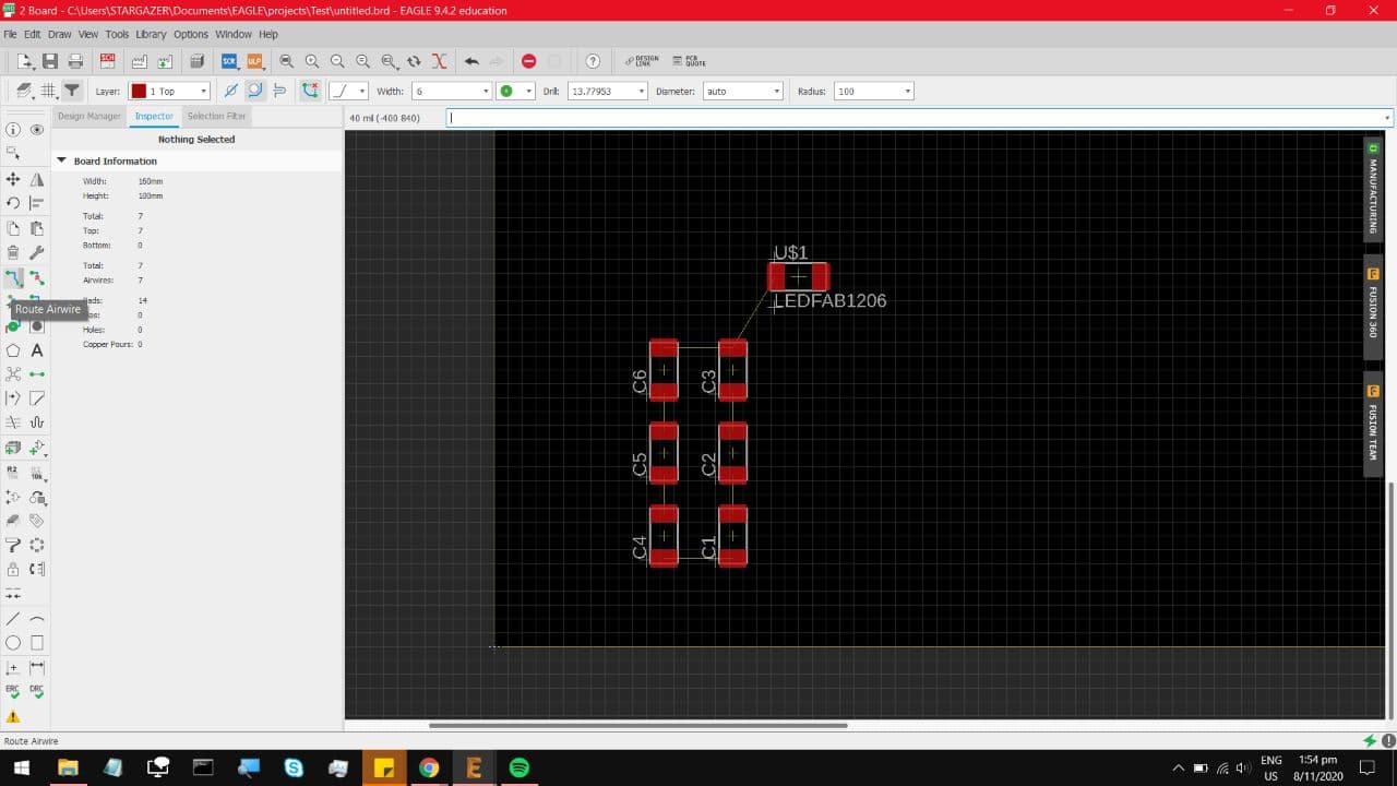
Next, try to move the entire pattern as close to the Bottom left corner of the work area, that bottom
corner is the origin. There is a tool highlighted, Route Airwire, select and use that to draw the Actual
circuit connections.
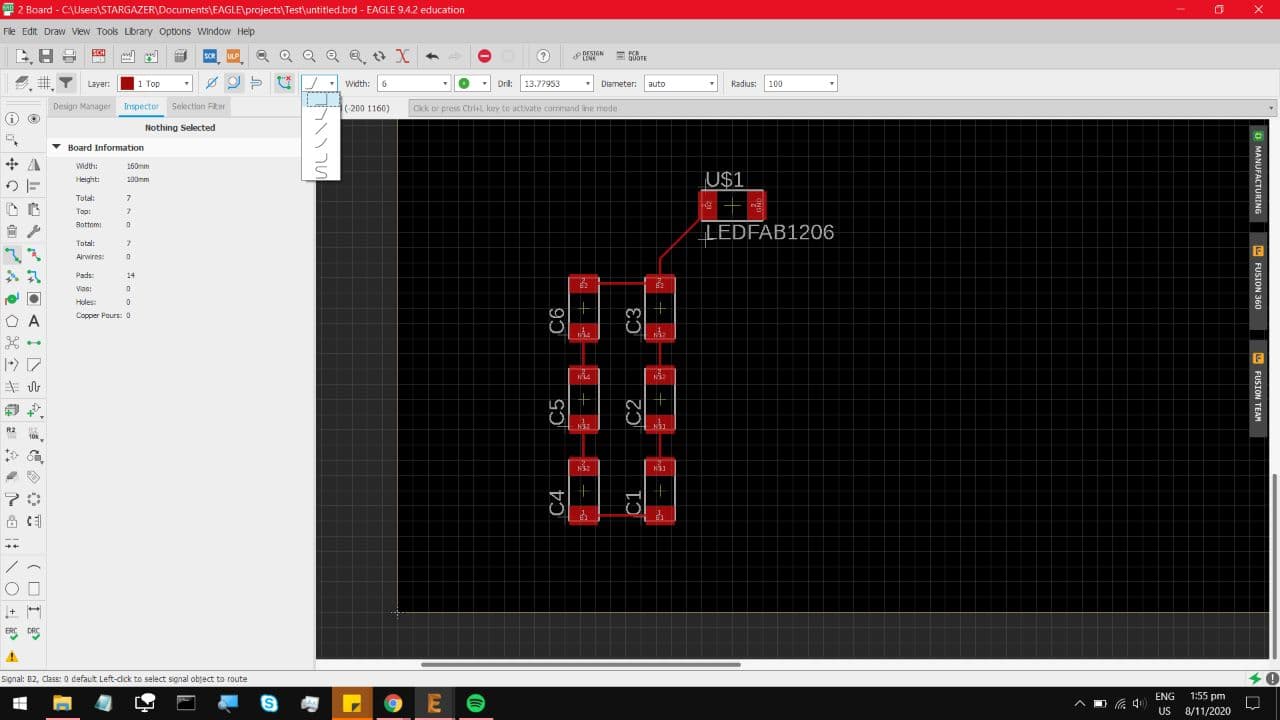
That is done for now, the tool highlighted in this one can select how the Routes deal with corners.
the default setting locks the corners to 45 degree angles because apparently Lithography does not cope
well with 90 degree corners. As for our method of production, a CNC router has no trouble with those
90 degree corners.
So now we are ready to capture the artwork, so go under Layers.
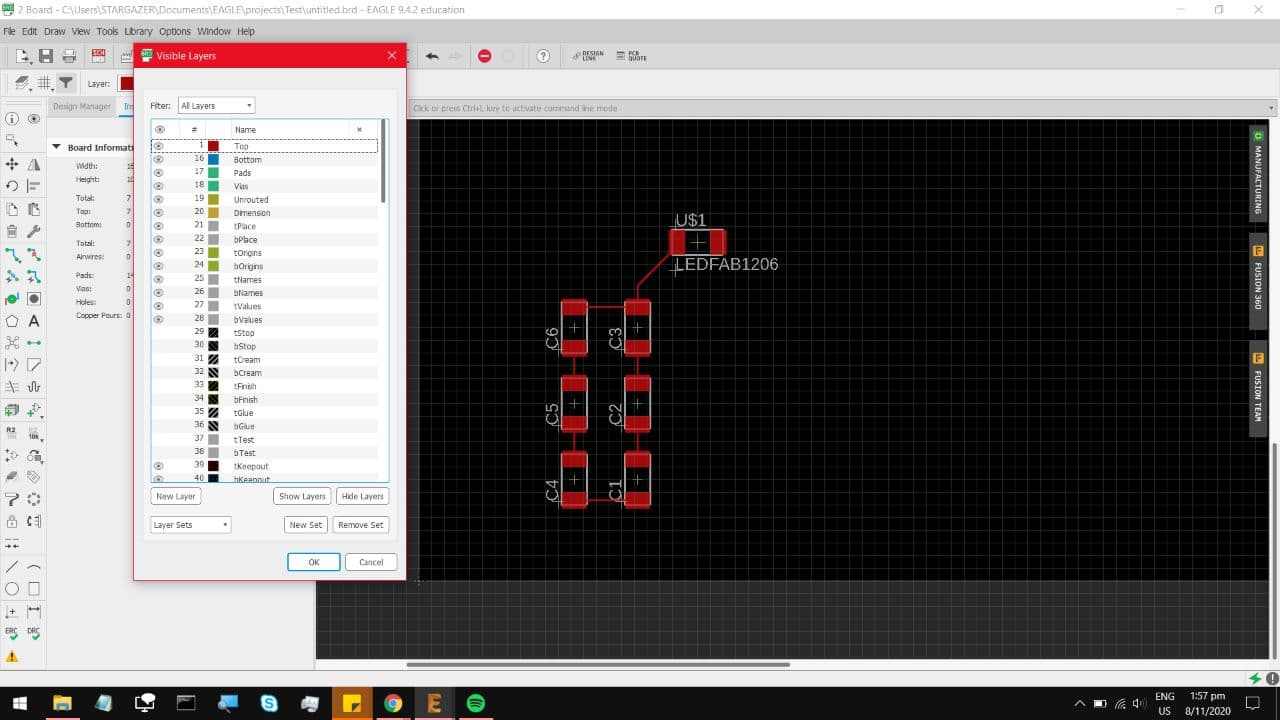
Select all layers, hide them, and unhide only the Top layer, this will show only the connections and pads.
Also don't forget to Resize the work area so your captured image later is not massive.
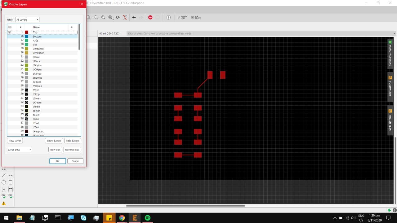
now with only the Top layer on, select Export, Image,
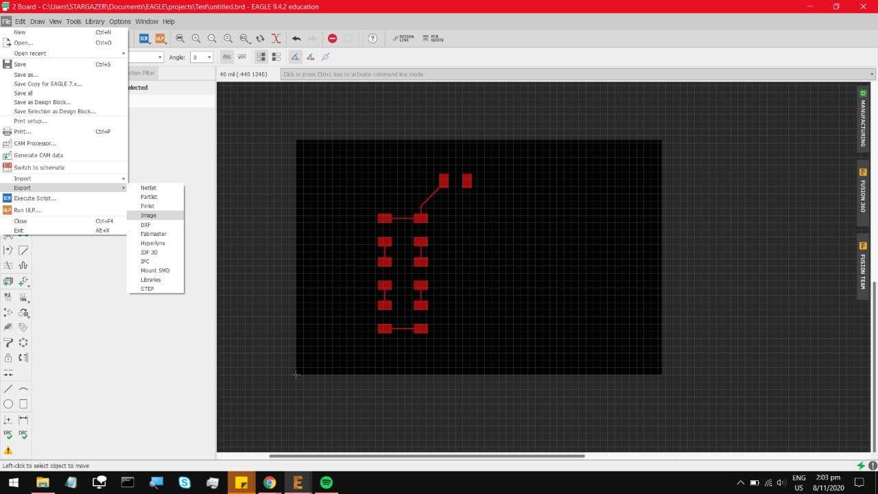
Name it, set the resolution up to about 1000, Monochrome, and hit Ok
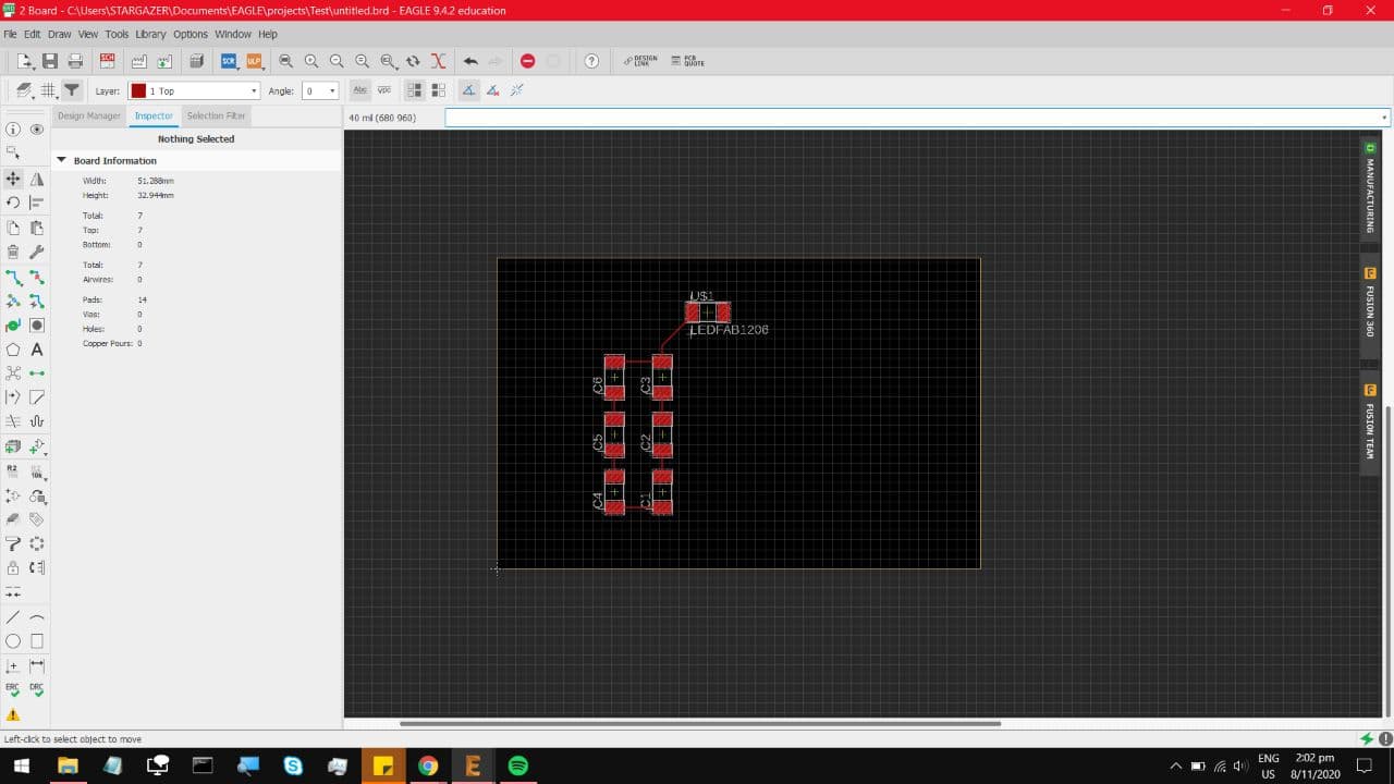
That circuit is fairly simple, when it comes to More complicated stuff, like This:
Your board ends up looking like this. Like I said, Labelling in important.
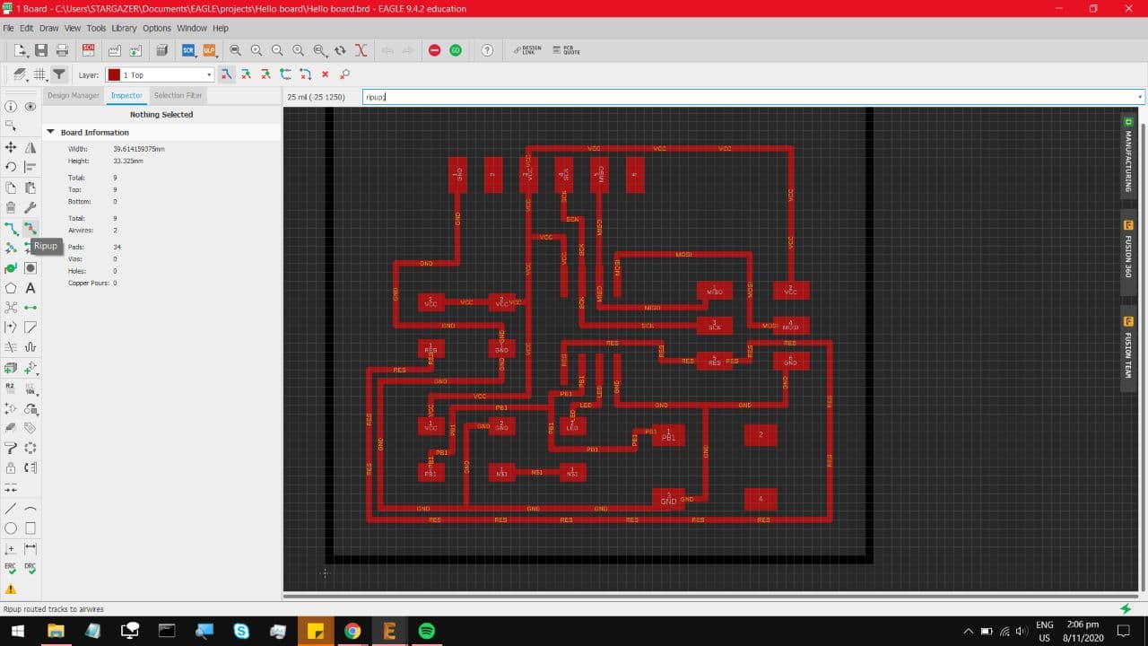
I missed out one thing before routing, which was to set the tolerances, but first,
That tool highlighted is Ripup, which erases the routes.
Alternatively you can type Ripup; in the command prompt to erase All routes.
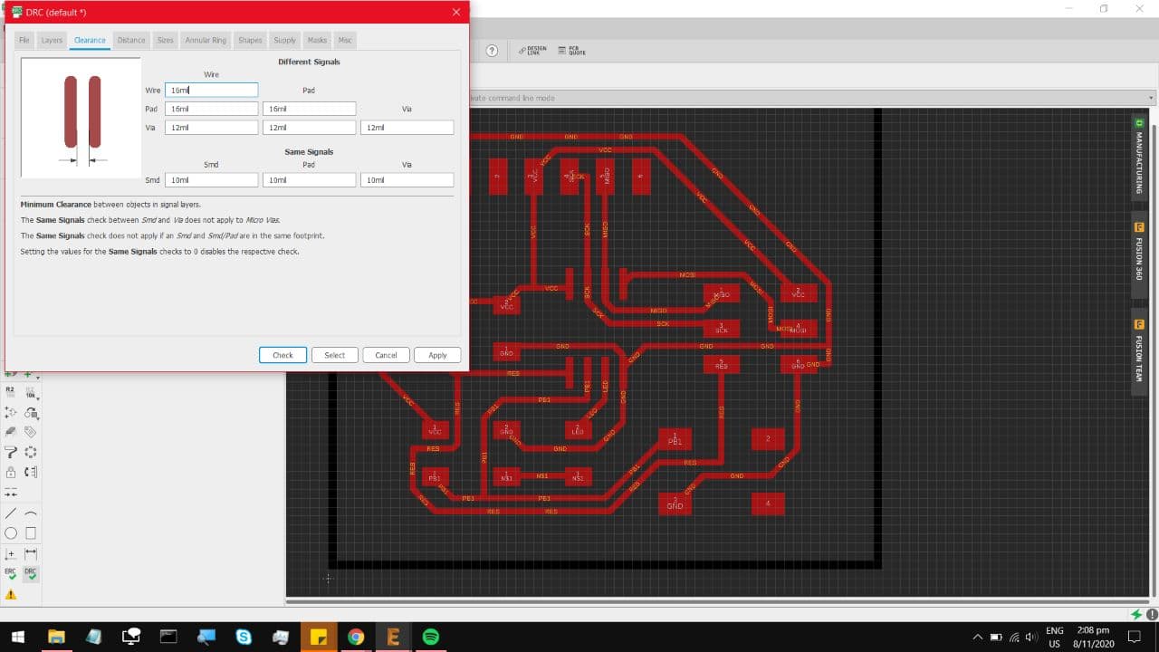
Which leaves us with this pattern, go under the DRC settings and look for Clearances. These
will help limit the minimum distance between each path so that it is possible to mill out with
a CNC router, Use these settings for the FabLab's router bits:
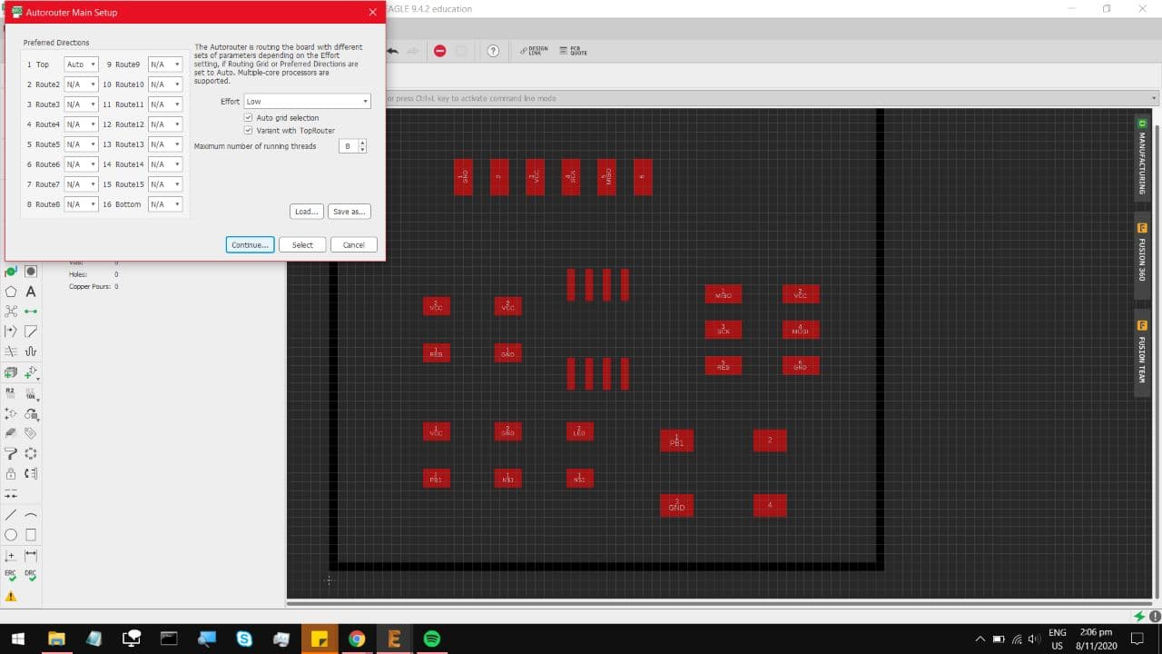
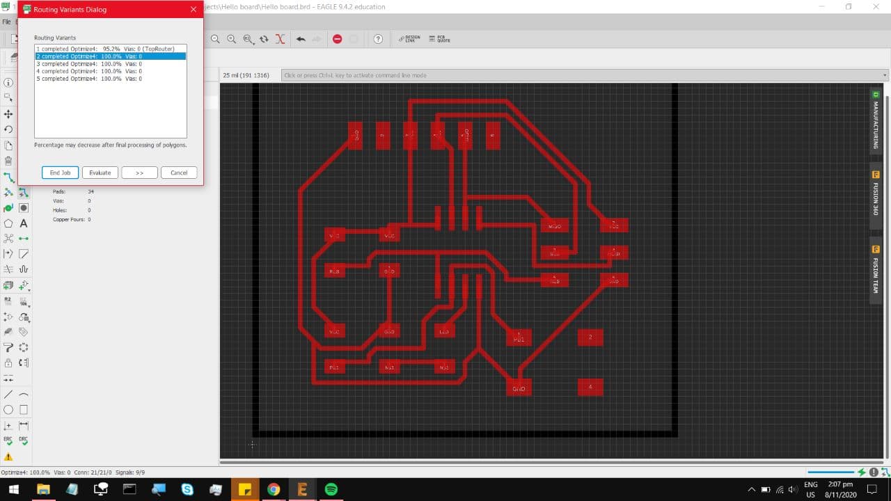
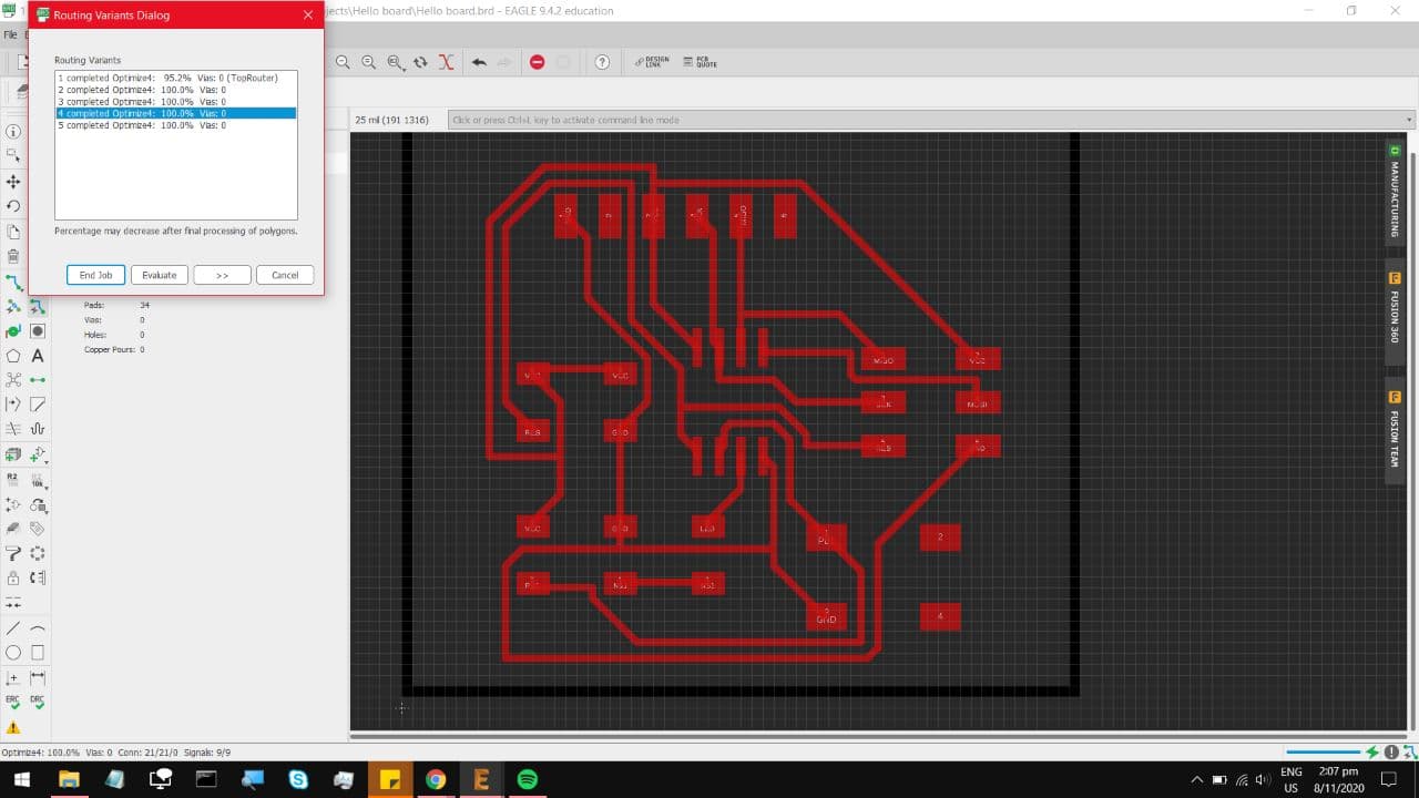
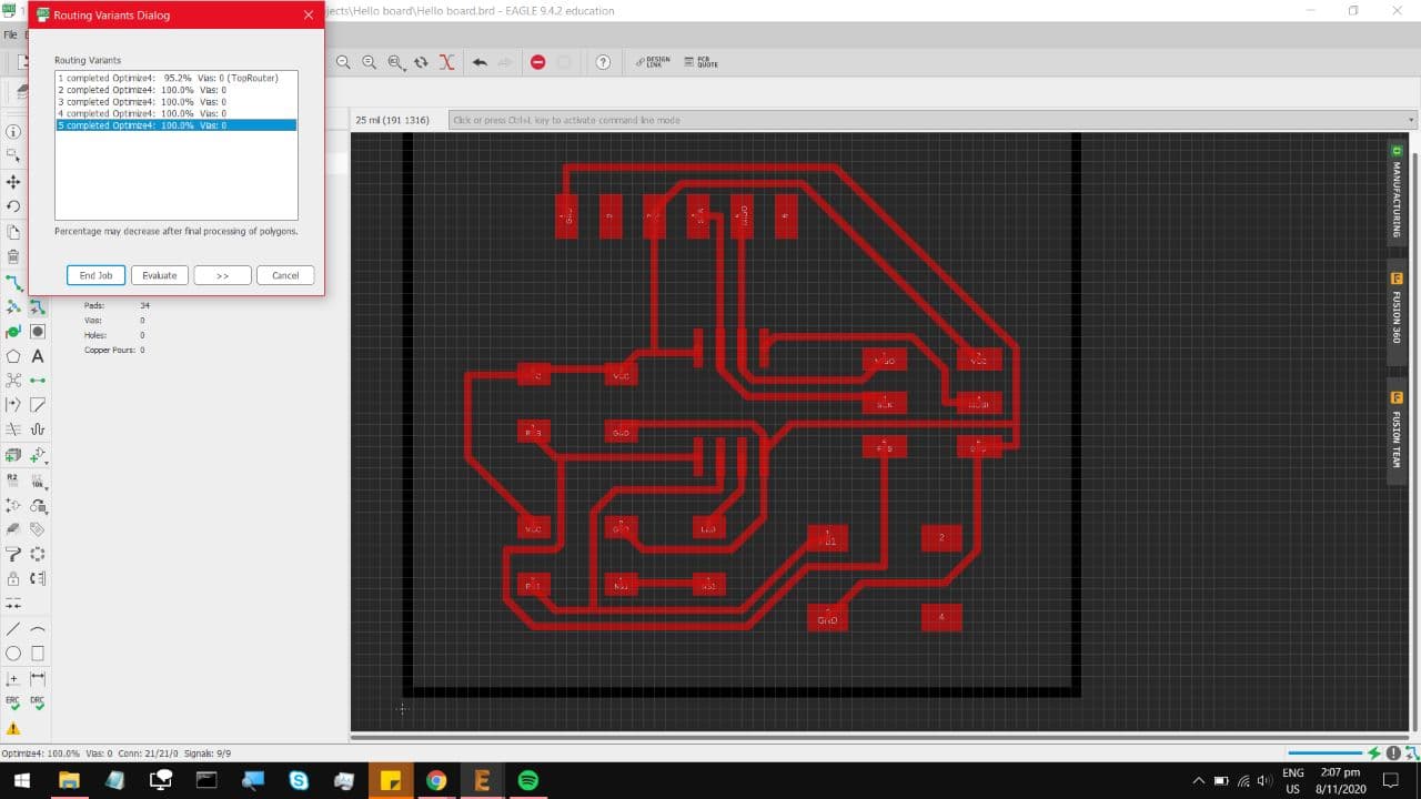
Now we can use something called Autorouter, and it does exactly what it says.
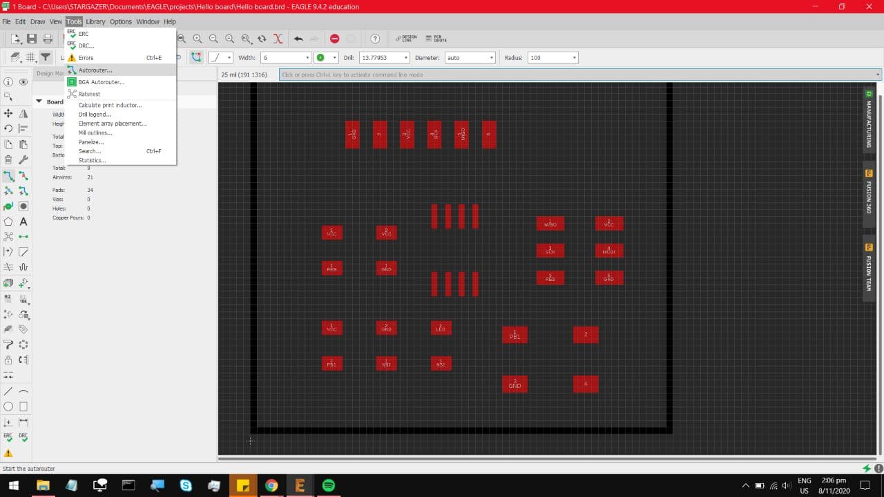
Configure those settings, such that it only worries about the Top Layers, and hit continue.
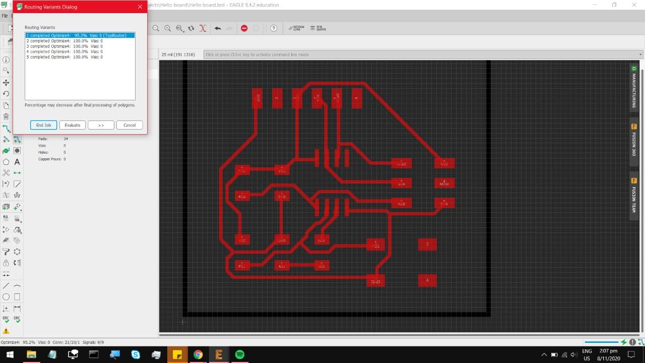
And now it will present to you the top 5 possible route patterns, which immediately look alot more professional.

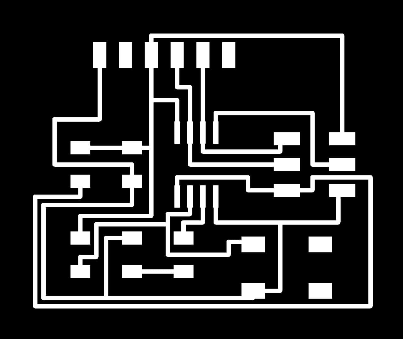
For this one I felt like doing things manually, so this is the exported trace and outline cuts

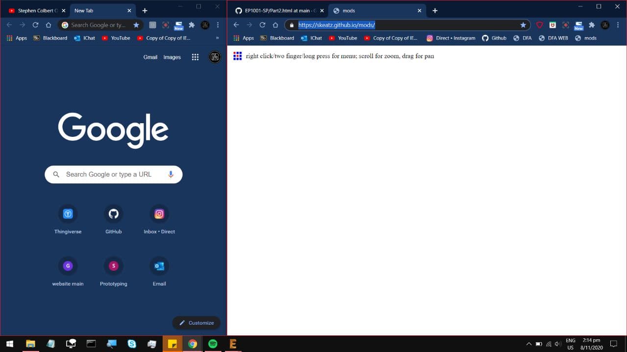
Once you have those exported, Open up this link:
That will take you here, this is Mods, cloned to a directory that might not change any time soon.
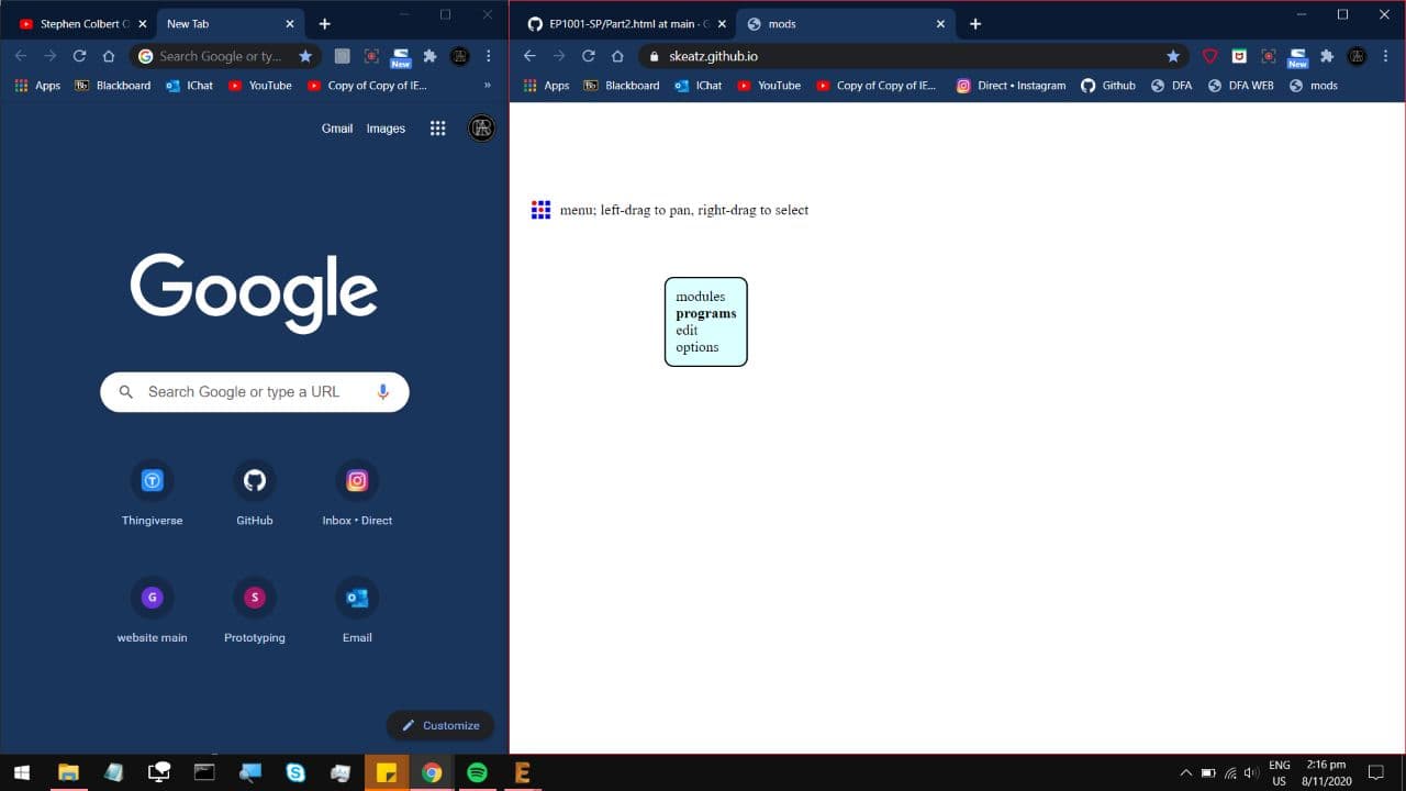
Right click anywhere, and select Programs,
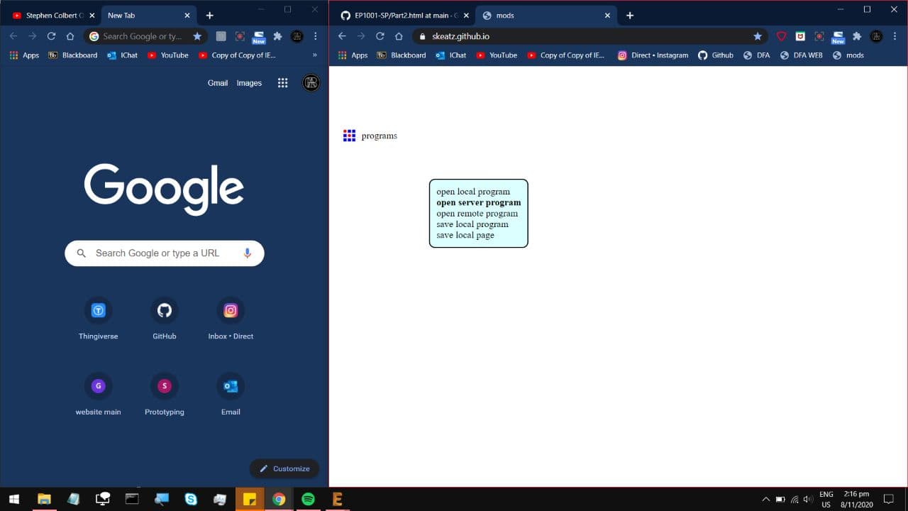
Select Open Server Program,
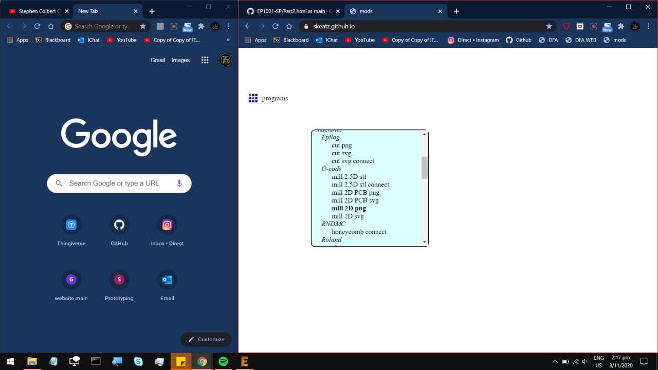
And under Gcode, select mill 2D PCB png
You'll be met with this monstrosity, you can ignore most of it and only touch a few things
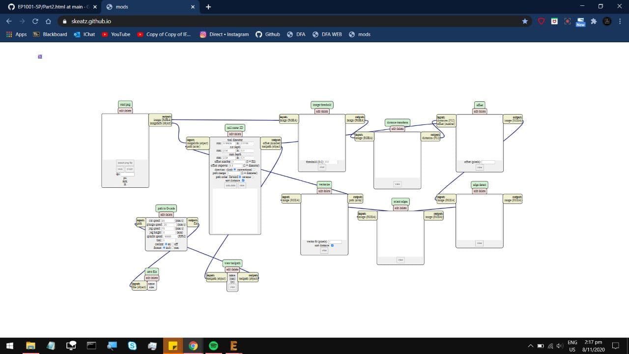
First, in the module on the top left, open your PNG file, if its the Traces, keep it with the routes white on a black
background. If its the Outline, invert it, such that its mostly white.
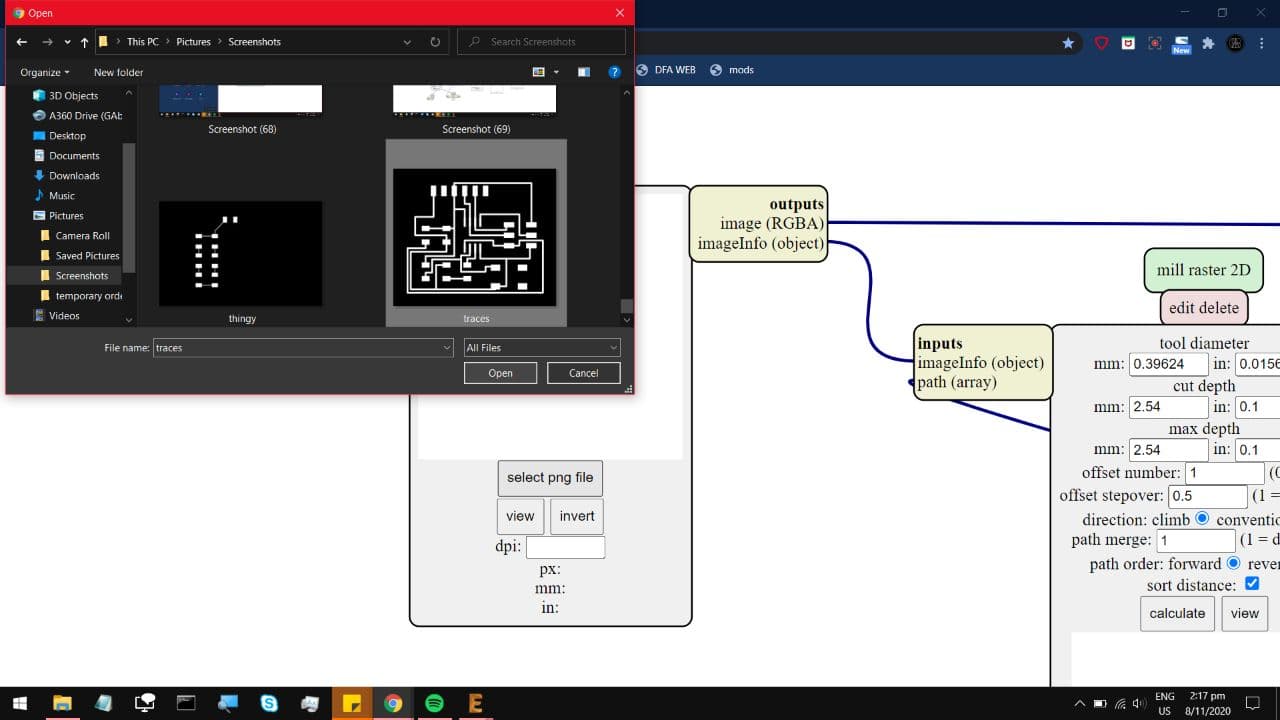
In the module next to it, input these parameters. For Offset number, that selects how many
times the path will be repeated, with an offset of around 0.5. The higher that number, the wider
the separation between each trace will be, which would make it easier to solder components onto.
However that also means the cycle would take much longer, and the traces might be more fragile.
I would go for at most 2 offsets, and even that is still pushing it abit too far with a v bit.
The bit used for the traces is 0.4mm and the one used for the outline is 0.8mm. To the bottom
left of that module, enter a cut speed of 50mm per minute, best case is to go slow and steady.
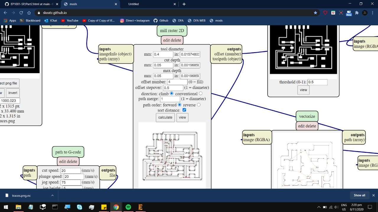
Once all that is ready, click calculate, and you'll have this show up, and the Gcode downloaded.
Now repeat this for your outline shape, I would recommend Inverting the colours, so you should end up
with a white silhouette of your ciruit board shape, with a black perimeter. Just be sure to change the
tool diameter to 0.8mm. Your minimum cut depth would be around 0.42, and the max being 1.67, offset 1.
What this will do is to trace the exact same outline, around 4 times, but sending the mill bit down by
about 0.4mm each time. This is far safer as it puts less stress on the very thin End-mill bit, shaving
off a small layer at a time, as opposed to driving the mill bit down 1.67mm and dragging it along the
copper blank, which will almost definitely sheer the bit in half, and put a nice hole into the board.
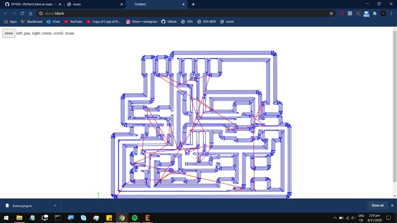
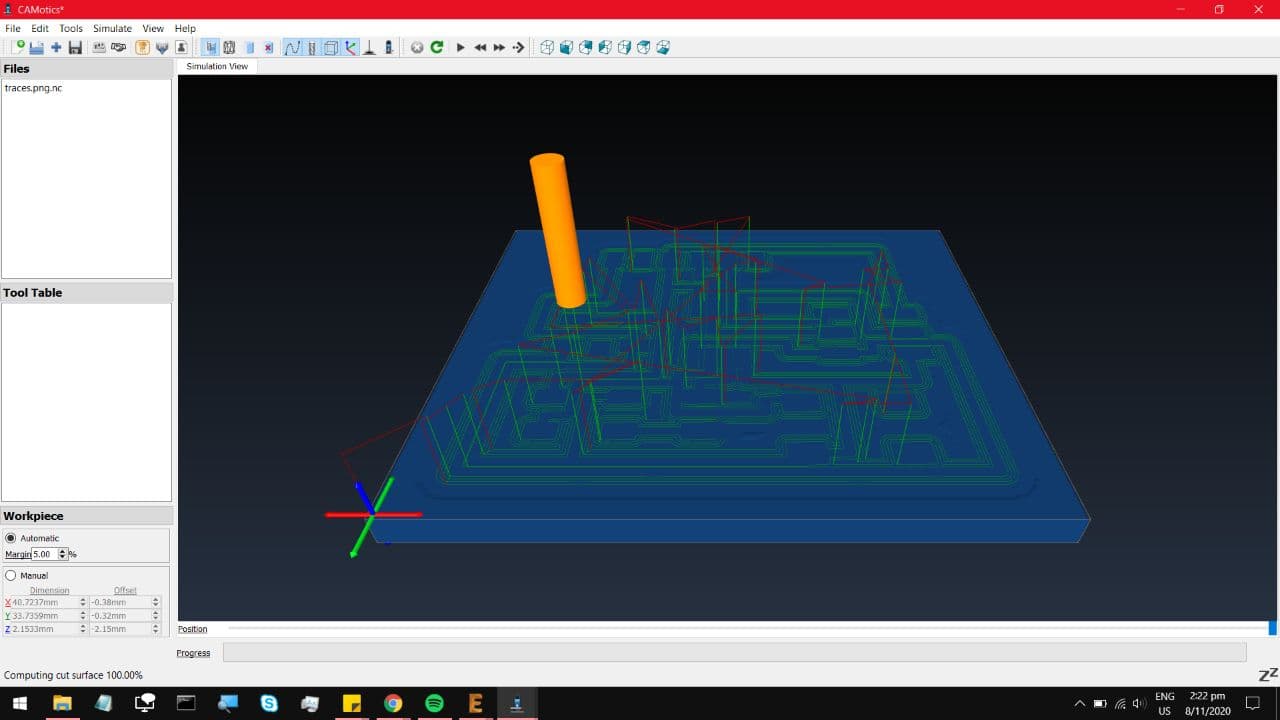
One additonal step would be to use Camotics to check the traceroutes for any issues.
Select Open project, and open the Gcode you just downloaded, and you will see something like this.
Look at the green path, that will be the path of the mill bit. It should be alright if the simulation
looks like its cutting away more than it should be, because the mill bit in real life is not nearly as
big as that orange peg moving around. Once you are satisfied, book a slot on the CNC router, and get cutting.
Interfacing & Applications Programming